
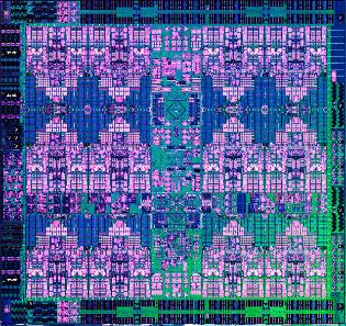
An open source AI inference SoC — 32 AI accelerator cores paired with a dedicated cluster of small POWER ISA control cores, dual PCIe Gen5 and OpenCAPI host interfaces, and card-to-card chaining. Single-slot, 75W. Sixteen cards per chassis where a GPU system fits eight. Entire SoC is POWER ISA — no RISC-V, no hybrid ISA, fully auditable from silicon to firmware.
Current AI inference deployments are built around large, hot, expensive GPU cards — designed for training workloads and repurposed for inference. A standard AI inference server holds eight double-wide GPU cards drawing 350–700W each. The chassis runs at 3–5 kilowatts. The hardware is proprietary, the firmware is unauditable, and the economics are controlled by a single vendor.
OpenAIU is designed from first principles as an inference accelerator. Single-slot. 75W. A standard server chassis that today holds eight double-wide GPU cards holds sixteen OpenAIU cards. The same rack space, at roughly one-quarter the power draw per inference node, running open source silicon with auditable firmware from boot to inference kernel.
The SoC uses two tiers of POWER ISA cores: a dedicated POWER Control Cluster of four Microwatt-class in-order cores handling on-card firmware, host bridge management, NOC orchestration, and power/thermal control — and a 32-core AI compute array connected to those control cores via the Auxiliary Execution Unit (AXU) interface. High-bandwidth memory access is delivered through an open OMI buffer. The entire SoC — control plane and compute — runs POWER ISA. No RISC-V, no hybrid ISA, no proprietary management microcontroller.
The project will use agentic EDA AI tools — Cadence ChipStack AI and Synopsys DSO.ai — to compress what would traditionally be a 5-year design cycle into a 36-month delivery.
Single-slot form factor at 75W fits 16 cards where a GPU-based inference server holds 8 double-wide cards. Same chassis, double the inference nodes, each independently managed.
At 75W vs 350–700W per GPU card, OpenAIU targets dramatically lower power per inference unit. Designed for sustained inference workloads — not peak GPU training bursts.
AI core RTL, control firmware, and memory interface are Apache 2.0 open source. Every numerical operation is specifiable and verifiable — critical for regulated AI deployment under EU AI Act and OCC model risk guidance.
Open RTL, open firmware, open toolchain. Any OPF member can manufacture, deploy, or extend the design. No per-card royalties, no driver licensing, no ecosystem lock-in.
Performance targets are architectural goals based on design parameters. Validated benchmarks will be published following FPGA bring-up at milestone M6.
Thirty-two AI accelerator cores arranged in an 8×4 grid, connected by a bidirectional ring bus. Each core contains:
The POWER control cluster exposes an Auxiliary Execution Unit (AXU) interface — a standardized connection point defined in the POWER ISA that allows custom functional units to sit directly adjacent to the POWER execution pipeline. AXU operations are dispatched as POWER ISA instructions and share register state with the control core's integer and floating-point register files. This means the AI cores in OpenAIU are not a separate "device" communicating over PCIe or even an AXI bus — they are execution units from the CPU's perspective, with register-speed data transfer and zero DMA overhead for small tensors. The POWER ISA Matrix Multiply Assist (MMA) instructions are specifically designed to dispatch to AXU-class functional units of exactly this type.
Modern AI accelerator SoCs commonly use a two-tier architecture: small management cores handle PCIe enumeration, DDR initialization, and NOC fabric orchestration, while the compute array handles the AI workload. It is the correct structural pattern — separating control plane concerns from compute plane concerns allows each tier to be optimized independently.
The typical industry choice for those management cores is RISC-V. OpenAIU makes a different choice: the control cores are Microwatt-class POWER ISA cores. This has three compounding advantages:
The four Microwatt control cores are small, in-order, and clocked conservatively — their job is orchestration, not compute. They consume a fraction of the die area and power budget. The AI compute array does the heavy lifting; the POWER control cluster makes the card a first-class, autonomously bootable, fully managed PCIe device.
OpenAIU supports two host interfaces — and this is the architectural feature that makes it viable across the broadest possible deployment base:
The two interfaces are not exclusive — the card negotiates at boot time based on what the host presents. The same hardware ships to an x86 hyperscaler over PCIe and to a POWER-based regulated industry deployment over OpenCAPI, with the on-card POWER control cluster managing interface initialization in both cases.
OpenCAPI's topology supports direct card-to-card communication without routing through the host CPU. Multiple OpenAIU cards can be chained into an inference fabric — sharing the KV cache for long-context inference, pipelining model layers across cards, or distributing batch workloads across the full card pool.
The Open Memory Interface (OMI) is a low-latency, high-bandwidth serial memory interface — a subset of the OpenCAPI specification — that delivers HBM-class bandwidth with a fraction of the die area of traditional parallel DDR interfaces. IBM uses OMI across POWER10, POWER11, and Spyre. The problem: every existing OMI buffer chip (the component that bridges the OMI serial link to LPDDR5 or HBM memory) is proprietary. Microchip Technology's explorer buffer chip is the only commercial option, and it is closed. OpenAIU requires an open OMI buffer chip as a sub-project deliverable. The path forward uses the Universal Memory Interface (UMI) from Zero ASIC as a transaction-layer reference, combined with an open-source SerDes implementation, to build a minimal OMI-compatible buffer in an accessible process node. This is explicitly the highest-risk deliverable in the project scope and is flagged for early funding prioritization.
A traditional silicon design project of this complexity — a multi-core AI SoC at 5nm — takes 5–7 years from architecture to tape-out. The OpenAIU project explicitly targets 36 months by using agentic AI-powered EDA tooling throughout the design flow. This is not hypothetical: the tools exist and are in commercial use as of 2025-2026.
Agentic AI that automates RTL coding, test plan generation, regression orchestration, and bug fixing for the Microwatt control cluster updates and AI core RTL. Announced February 2026. Compresses front-end design from months to days for well-specified blocks.
Autonomously reaches coverage targets up to 10× faster by identifying redundant tests and routing simulation resources toward uncovered functional states. Critical for verifying AI core correctness and AXU dispatch correctness across all precision formats.
Uses reinforcement learning to optimize floorplanning, clock tree synthesis, and power gating across all 32 AI cores simultaneously — targeting the 75W envelope with up to 20% better power efficiency than manual closure. One engineer can drive multiple block closures in parallel.
Autonomous search across the implementation design space (synthesis strategies, placement constraints, routing options) to find minimum-power configurations at 5nm. Particularly valuable for the AI core array where repeated instances allow aggressive optimization sharing.
For the analog-intensive open OMI SerDes and memory interface circuits. AI-assisted process migration takes an existing open-source SerDes design and retargets it to the 5nm node, dramatically reducing analog design iteration time — the slowest part of any mixed-signal SoC.
The AI core array and the Microwatt control cluster may be implemented as separate chiplets (AI cores at 5nm, control cluster at 7nm) connected via UCIe die-to-die interface. This reduces per-die yield risk and allows node-optimized manufacturing for each functional block. AI-driven EDA tools optimize the die partition boundary.
Regulated industries deploying AI for credit decisions, fraud detection, clinical decision support, or benefits eligibility face a specific problem with current AI accelerator hardware: the inference computation is performed on opaque proprietary silicon with no auditable firmware and no independent verification of numerical precision. Regulators in the EU (AI Act), US financial sector (OCC guidance on model risk), and healthcare (FDA guidance on AI-based devices) are increasingly focused on infrastructure provenance for AI systems.
OpenAIU is designed with auditability as a first-class architectural requirement:
OpenAIU is not a standalone device. It is designed as a component in the full ESI stack:
| Parameter | Specification | Notes |
|---|---|---|
| AI Cores | 32 (8×4 grid) | Open RTL, 2D systolic + 1D vector per core |
| Precision | INT4 / INT8 / FP16 / BF16 | Hardware acceleration for all; INT4 for LLM inference |
| On-chip SRAM | ≥64 MB | Distributed tiles + shared L3 |
| Memory Interface | OMI (open buffer) | OpenCAPI OMI subset; LPDDR5X memory stacks |
| Memory Bandwidth | >200 GB/s | Peak to AI core array |
| Control Processor | 4× Microwatt POWER ISA | AXU-coupled to AI array; MMA instruction dispatch; full POWER ISA |
| Host Interface | PCIe Gen5 ×16 / OpenCAPI | Negotiated at boot; OpenCAPI primary on POWER hosts; PCIe fallback for x86/ARM |
| Power Envelope | 75W TDP | PCIe card form factor, passive or active cooling |
| Process Node | 5nm (TSMC N5) | 7nm fallback; chiplet option for mixed nodes |
| Architecture | Monolithic or 2.5D chiplet | UCIe die-to-die interface for chiplet variant |
| Firmware | Open source (Apache 2.0) | Boot via OpenFSP; management via OpenHMC |
Published microarchitecture specification for a single AI core: systolic array dimensions, vector unit design, SRAM tile, and AXU dispatch protocol. Month 4.
Synthesizable open source RTL for the full 32-core array including ring bus interconnect. Verification suite with INT4/INT8/FP16/BF16 test vectors. Month 14.
Open source OMI buffer chip design — the most novel deliverable. SerDes, memory controller, and OMI protocol stack. FPGA-verified. Month 18.
Microwatt control cluster + AI array + OMI + PCIe Gen5 + OpenCAPI integrated into a complete SoC RTL. Functional simulation with reference AI models (BERT, LLaMA quantized). Month 22.
Partial implementation on UltraScale+ — Microwatt control cluster + reduced AI core array (8 cores) — running quantized inference against reference benchmarks. Month 20.
GDSII at 5nm (or 7nm). PPA closure verified with Cerebrus/DSO.ai. DRC clean. Third-party security audit of AI core arithmetic. Month 36.
Every major regulated industry is deploying AI inference on-premises — for model risk compliance, data residency requirements, or latency-sensitive applications. They are doing it on proprietary GPU hardware they cannot audit, connected via proprietary software stacks they cannot verify, managed by cloud providers whose infrastructure they cannot inspect.
OpenAIU is the only project in the world combining: an open processor ISA with IBM patent coverage, open AI accelerator cores derived from published research architecture, auditable firmware from chip boot to inference kernel, and a hardware form factor compatible with multi-vendor manufacturing. For a bank that must explain to its regulator exactly what hardware and software computed a credit decision — OpenAIU is infrastructure that makes that explanation possible. No proprietary GPU can.